Sony and TSMC sign MOU for a next-gen image sensor joint venture in Kumamoto, marking Sony's first step toward a fab-light model.

www.cined.com
For decades, Sony has been the dominant force in CMOS image sensor design and manufacturing, supplying its sensors to most of the smartphone industry (including Apple, Samsung, and Huawei flagship devices), to most of its competitors in the camera industry, and of course to its own Alpha and Cinema Line cameras. The Imaging & Sensing Solutions division generated roughly $11.8 billion in sales in fiscal 2024 and remains the largest single recipient of Sony’s R&D spending. The image sensor business is, in other words, not a sideline; it is one of the most strategically important units in the entire Sony Group.
That makes the framing CEO Hiroki Totoki used on the company’s post-earnings call notable. According to a Bloomberg report, Totoki told analysts that “the joint venture with TSMC will be our first step to becoming fab-light,” adding, “until now, we have handled everything in-house, from R&D to manufacturing, but going forward, we hope to advance manufacturing not only on our own but also by bringing in partners.” That is a meaningful change in posture from a company that has historically guarded its sensor manufacturing tightly.
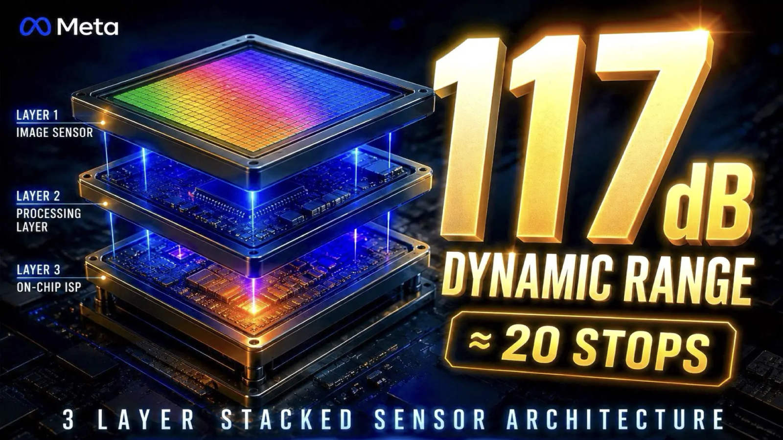
The strategic logic, read between the lines, is straightforward. Modern stacked CMOS sensors (the kind that power cameras like the Sony BURANO, the a7 V, and the recently announced
LYTIA 901 smartphone sensor) are increasingly difficult and expensive to fabricate. They require precise wafer bonding, on-chip logic and AI processing circuits, multiple stacked layers, and yield rates that fall as complexity grows. TSMC has spent a generation building exactly the advanced process technology and capacity that next-generation image sensors require. Bringing TSMC inside the tent gives Sony access to that capability without having to build (and finance) every new fab from scratch.